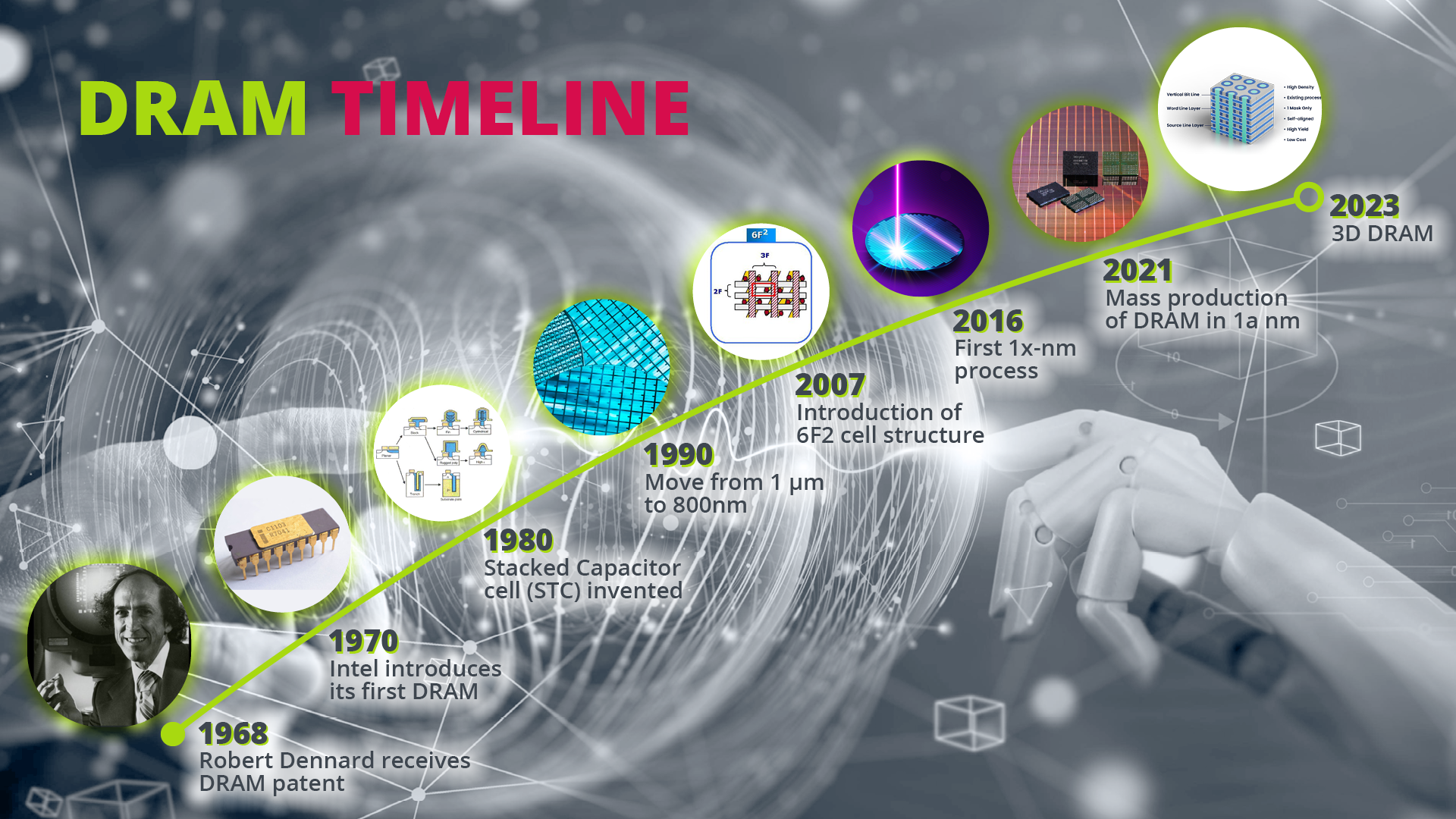
On June 4, 1968, Robert Dennard was granted a patent for a single transistor, single capacitor DRAM cell design idea. This doesn’t sound earth-shattering today, but back in the sixties, this was a radical new approach.
Because when he set out in 1966, Robert Dennard was trying to create an alternative to SRAM and magnetic core memory which required either six MOS transistors for each bit of data or a semi-hard ferrite core ring. His observation that MOS technology was capable of building capacitors led him to the conclusion that one transistor and one capacitor would be all it needed for a memory chip. This simple structure is still how DRAMs are set up today.
As early as 1969 Advanced Memory System commercialized its first MOS DRAM chips but sold the 1024-bit chip to Honeywell which in turn asked Intel to make a DRAM based on a three-transistor cell that it had developed. Due to the many issues of this three-transistor 1102 DRAM, Intel worked on its own design and introduced its first i1103 DRAM in October 1070 which was the first commercially available and successful DRAM IC.
How does DRAM work?
But even though the 1 transistor 1 capacitor structure is very simple, DRAM had its teething troubles. In fact, the first five DRAM generations that Intel introduced had a very low yield as the analog behavior of the DRAM cell only started to reveal. While the memory cell itself contains a digital signal (0 or 1), in order to produce a digital signal, an analog signal must be read out, amplified and written back. To understand what this means, lets look at the DRAM structure.
DRAM cells are laid out in a regular rectangular, grid-like pattern to facilitate their control and access via wordlines and bitlines and sense amplifiers are required to read the state contained in the DRAM cells. After initial amplifaction, the signals need to be transferred quickly over a long distance on chip again requiring a second analog sense amplifying process. When the access transistor is activated, the electrical charge in the capacitor is shared with the bitline. The bitline's capacitance is much greater than that of the capacitor (approximately ten times). Thus, the change in bitline voltage is minute. Sense amplifiers are required to resolve the voltage differential into the levels specified by the logic signaling system. This is all a very analog behavior.
But what the initial DRAM designers had to get their head around was problems like the propagation delay in connecting and sensing the cells which needs to be timed precisely in an analog fashion considering the slowest cell at the farthest away spot. If timing is not correct and too early or too short signals can flip into the wrong direction or there is too weak signal written back into the storage cell.
It took detailed analysis from a couple of test, design and product engineers to solve these problems, but after that, the success story of DRAM began. The intel i1103 was also called the “core killer” since it was so successful in replacing traditional ferrite core-based memory cells.
Scaling is everything
When I started in the semiconductor industry in the late 80s we were working on DRAMs in a 5000-nm process. An assistant would print out the masks, or rather plotted them on foils, and we scaled them down by factor 100 with a simple camera. Today we are at a 12-nm process and the slightest contamination can impact the etching and destroy cells.
The scaling we have seen in the past years is nothing but amazing. Intel’s 4004 processor operated at 740kHz, that’s 2 million times slower than today’s processors and DRAM interfaces. Today we have densities of up to 16Gb (mono-dies), that is 16 million times more than the first DRAM.
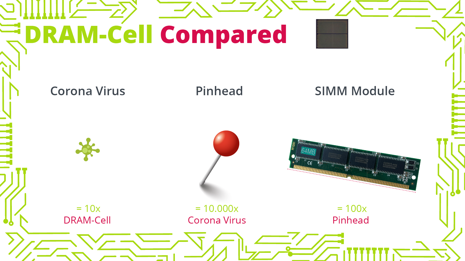
Did you know that with today’s processing nodes, you can squeeze 10 DRAM cells in 1 coronavirus? Today memory cells are so small that they can only contain 10,000 electrons. They are tiny, delicate structures that have to be heaved to crude bit lines to check if their load is 0 or 1. With this in mind, it’s actually a little miracle that they work reliably and that DRAM and flash memory roughly constitute 30% of all semiconductor sales in the world. Today they are operating for years in Mars-based rovers, landing equipment on comets and basically being part of all electronic equipment on earth.

In the early days of 1,000 DRAM cells per memory IC it was fairly easy to ensure that all of the cells worked correctly. Today we have up to 16 billion cells on a die and need error correction to repair the cells that fail and even that doesn’t catch all faults. With lithography reaching its physical limits, every single DRAM runs through about 10 hours of testing in the various stages of its creation. However, there are errors in DRAM technology that only arise in longer run times or in its use case.
To Fail or not to Fail
I remember a case where DRAMs failed, but the manufacturer couldn’t replicate the failure to identify the source. After a while engineers found that some cells lost their charge when radiation hit them. However, this only happened occasionally when radiation was emitted on chip and hit the memory cells with right incident angle. It took almost a year to trace this behavior back to the wafter production where one manufacturing line used water with a slight radioactive contamination.
But fails don’t always track back to the manufacturing process. DRAMs have also become the target of cyber-attacks. A couple of years ago hackers found out that by activating the same memory rows in DDR3s over and over again, they can leak charges or possibly change the contents of a nearby memory row. This was the first time the high density of cell rows in a memory had been exploited for an attack (row hammer attack). Memory manufacturers had to do quick fixes by lowering wordline resistance and other measures. Final fix in later DRAM designs is to issue extra refresh cycles during such situations preventing the row hammer effect without negatively impacting normal performance or power consumption.
All these are results of extensive testing. While testing has been an important aspect of bringing DRAM to market, these examples show that testing is more important than ever today. The more complex the manufacturing process of DRAM gets and the more specialized its application is, the less you can predict how a DRAM will actually do in the target application without extensive application-specific testing. In addition, increasing clock and data transmission speeds cause more and more signal integrity issues in applications that are not flawlessly designed. As most manufacturers stick to their conventional standard tests, we fill the gap with our new DRAM test board that can simulate actual application environments.
What’s next?
3D DRAM is hailed as the next big thing. But seeing the challenges we are facing with the evolution of memory transistor devices and the extreme requirements for super low leakage DRAM requirements I can hardly see how this will happen any time soon. We’ve been trying to find a stacking solution in the 30 years I have been in the business. Stacking is easier in flash as you are dealing with poly-crystalline silicon and have now low leakage or stringent floating transistor requirements. FLASH principal is simply based on a shift of threshold voltage by trapped charges. In DRAM you need monocrystalline structures with a flawless low leakage behavior and no floating bulk to perfectly switch of the memory cell transistor.so the DRAM can turn off with minimal leakage to hold the charge for 64ms.
But 3D DRAM still inspires engineers to come up with new approaches, and we will see pretty soon if a 3D DRAM will make a breakthrough. Because after all, the past 55 years have shown the boundless innovation power in DRAM.
Author: Dr. Peter Pöchmüller, CEO of Neumonda

Note: This is a repost of an article published on embedded.com


